(China (Mainland))

Product Summary
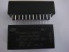
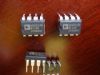
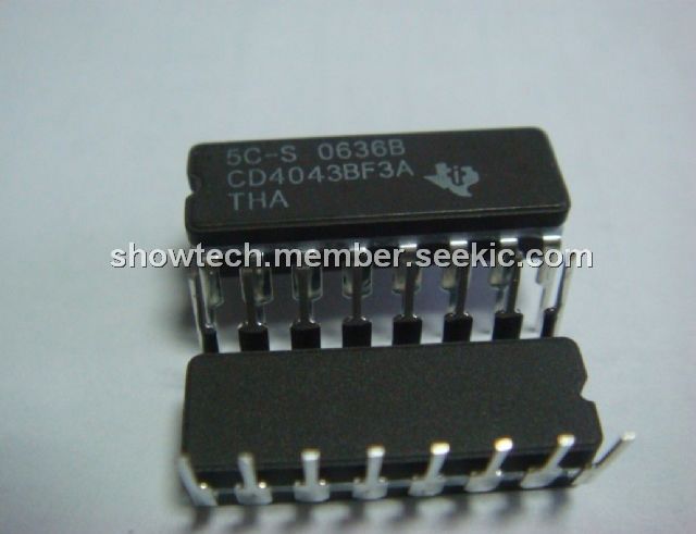
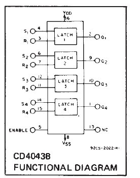
The CD4043BF3A is a quad cross-coupled 3-state CMOS NAND latch. The CD4043BF3A has a separate Q output and individual SET and RESET inputs. The Q output is controlled by a common ENABLE input. The applications of CD4043BF3A are: (1)Holding register in multi-register sysytem; (2)Four bits of independent storage with output enable; (3)strobed register; (4)General digital logic.
Parametrics
CD4043BF3A absolute maximum ratings: (1)DC supply-voltage range, VDD: -0.5 to +20 V; (2)input voltage range, all inputs: -0.5 V to VDD+0.5 V; (3)DC input current, any one input: ± 10 mA; (4)power dissipation per package: 500 mW; (5)device dissipation per output transistor for TA=fullpackage-temperature range: 100 mW; (6)operating temperature range: -55 to +125℃; (7)storage temperature range: -65 to +150℃.
Features
CD4043BF3A features: (1)3-state outputs with common output ENABLE; (2)seperate SET and RESET inputs for each latch; (3)NOR and NAND configurations; (4)5-V, 10-V and 15-V parametric ratings; (5)standardized symmetrical output characteristics; (6)100% tested for quiescent current at 20 V; (7)maximum input current of 1 μA at 18 V over full package temperature range: 100 nA at 18 V and 25 ℃.
Diagrams
 |
 CD4000B |
Other |
|
Data Sheet |
Negotiable |
|
||||
|
CD4000BMS |
Other |
|
Data Sheet |
Negotiable |
|
||||
|
CD4001BC |
Other |
|
Data Sheet |
Negotiable |
|
||||
 |
CD4001BCM |
|
IC GATE NOR BUFF QUAD 2IN 14SOIC |
Data Sheet |
Negotiable |
|
||||
|
CD4001BCMX |
|
IC GATE NOR QUAD 2INPUT 14-SOIC |
Data Sheet |
Negotiable |
|
||||
 |
CD4001BCN |
|
IC GATE NOR BUFF QUAD 2IN 14-DIP |
Data Sheet |
Negotiable |
|
||||